 Products Home / Custom Solutions & Manufacturing Capabilities / Optics Capabilities / Crystalline Mirror Coatings
Crystalline Mirror Coatings
- High-Reflectance Optical Coatings for 900 nm to 5.0 µm
- Coated Diameters Up to Ø200 mm with Custom Geometries
- Adhesive-Free Direct Bonding to Curved or
Planar Substrates
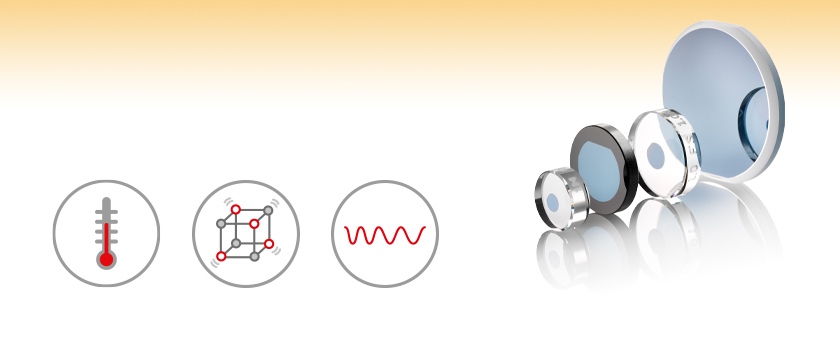
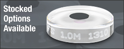
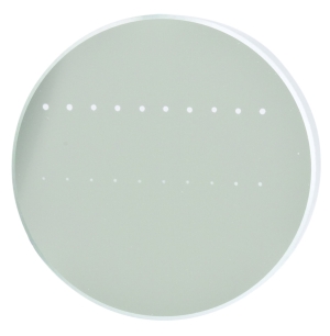
A selection of optics coated with our crystalline mirror coatings.
Lower Thermal Resistivity*
Lower Brownian Noise*
Lower Mid-IR Absorption*
*When Compared to Sputtered Amorphous Thin-Film Coatings


Please Wait
 Click to Enlarge
Crystalline mirror coatings exhibit lower mechanical noise than amorphous coatings. (Cole, GD et al., 2013. See the Publications tab for more details.)

Garrett Cole
Technology Manager,
Feedback?
Questions?
Need a Quote?

2017 Materials and Coatings
Features
- Single-Crystal GaAs/AlGaAs Optical Coatings
- High Reflectance from 900 nm to 5.0 µm
- Direct Bonding to a Variety of Substrates
- Low Optical Absorption and Scatter
- Low Thermal Resistivity
- Available from Stock in Plano and Concave Geometries
Applications
- High-Finesse Laser Cavities
- Low-Noise Precision Interferometry
- High-Power Laser Systems
- Mid-IR Spectroscopy
- Ultrastable Lasers for Atomic Clocks
- Mirrors for Gravitational Wave Detection
Thorlabs Crystalline Solutions offers high-performance, single-crystal mirror coatings and novel manufacturing processes tailored to meet your unique requirements. Our expertise in optical system design and advanced microfabrication techniques, including adhesive-free direct bonding services, enables the production of ultra-high-performance optical devices and systems.
We offer three varieties of our GaAs/AlGaAs coating, each designed to excel in a particular area: xtal stable™ for low Brownian noise, xtal mir™ for low mid-infrared absorption, and xtal therm™ for low thermal resistivity. Our adaptable coating process and expertise in direct bonding can be used to create custom coating designs and heterogeneous integrations for your application. Mirror coatings can be etched in arbitrary geometries and bonded directly to a wide array of planar and curved substrate materials. Contact one of our Tech Support engineers to discuss your crystalline mirror application needs.
Monocrystalline semiconductor materials like GaAs/AlGaAs exhibit quasi-bulk properties and lower mechanical noise than amorphous, dielectric coatings created from sputtering, as shown in the graph above. This is thanks to a nearly flawless crystal lattice created by molecular beam epitaxy (see the Technology tab for details).
Mirrors with crystalline coatings can be used to build high-performance single-element laser optics as well as complete laser cavities. We offer complete reference cavity assembly services including mirror coating, spacer acquisition, optical contacting, and testing. For more information, please see our High-Finesse Cavities tab. Mirrors and laser cavities like these have become key components in a wide variety of laser-based applications thanks to their low noise and high reflectance. Click here to view our select offering of plano and concave xtal stable™ mirrors available from stock.
Ultra-Precise Measurements of Space and Time
With our proprietary crystalline coating technology, we can construct optical cavities capable of significantly improved thermal noise performance. Mirror assemblies produced with our single-crystal mirrors offer a 10 times reduction in thermo-mechanical (i.e., Brownian) noise compared to amorphous mirror coatings deposited with sputtering. This substantial reduction in thermal fluctuations enables a significant improvement in the overall frequency stability of optical reference cavities.
High-Power Laser Cavity Construction
High-power lasers are limited by the unavoidable residual absorption of their reflective optics. The low thermal conductivity of sputtered coatings (on the order of 1 W/(m • K)) limits the effectiveness of any heat sink solution and attempts to avoid heat-induced structural damage in both the coating and laser system. GaAs/AlGaAs DBRs exhibit a thermal conductivity at least 30 times greater than traditional sputtered coatings. This significant performance improvement makes substrate-transferred crystalline coatings an ideal choice for optical systems requiring superior thermal management.
High-Resolution Trace Gas Sensing
Compared to typical dielectric materials, GaAs/AlGaAs-based interference coatings can achieve much lower optical losses in the important spectral MIR region between 2 and 5 μm, with absorption losses below 10 ppm. In first tests using substrate-transferred semiconductor materials, performed in the Ye group at JILA/NIST (see the Publications tab), a cavity with a finesse exceeding 10,000 was demonstrated, while simultaneously exhibiting a cavity reflection contrast of 71%.
 Click to Enlarge
 Click to Enlarge
 Click to Enlarge
 Click to Enlarge
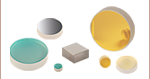
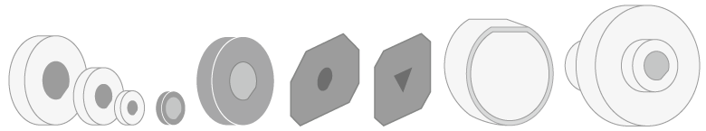 Substrates and coatings can be made to a variety of arbitrary geometries.
 Click to Enlarge
Garrett Cole, founder of CMS, inspecting a completed bond.
Production and Coating Technology
Molecular beam epitaxy (MBE) is a time-proven vacuum deposition technique traditionally used to create semiconductor structures. This process provides deposition rates on the order of single-molecular layers, uniformly distributed across a substrate. By leveraging the precision and accuracy of MBE, we can deposit high-purity single-crystal GaAs/AlGaAs multilayers with low defect density, generating optical interference coatings. Once qualified, these coatings can be released from its sacrificial wafer and bonded to one of a wide range of substrates.
The key to our crystalline coating lies in the fact that GaAs and AlGaAs have extremely similar lattice constants over a wide temperature range. By using a GaAs wafer as a substrate, it serves as a crystal template for the entire coating. The result is a single crystal with higher structural rigidity than amorphous solids on a molecular level. Lattice matching removes interlayer stresses as well as decreasing the frequency-dependent noise power spectral density (NPSD). NPSD is directly proportional to the loss angle of a material system, found in the complex form of the Young's Modulus. This relationship is explored in Cole, GD et al., 2013; see the Publications tab for more details.
Combining the precision of MBE with the unique properties of these materials, we are able to create mirror coatings with an engineered reflectance greater than 99.99% and total scattering and absorption losses under 5 ppm in the near-IR.
1. Coat
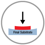
GaAs/AlGaAs multilayers are deposited on a sacrificial GaAs wafer as a precursor to direct bonding, which provides a near-perfect template for the crystal lattice to grow. This is in contrast to many traditional thin-film coating techniques, which deposit an amorphous coating directly onto the final substrate.
2. Test

By growing crystalline coatings on sacrificial wafers, each coating can be independently validated for optical performance and surface quality before being bonded to a final substrate. As opposed to other techniques, this process prevents substrates from being scrapped due to coating flaws.
3. Release

Once a coating is verified to meet the desired specifications, its geometry is precisely defined using lithography and etching techniques. The coating is then released from the GaAs wafer. Our coatings have been as small as Ø20 µm to as large as Ø200 mm with any arbitrary geometry in between.
4. Bond
Our proprietary direct bonding process enables dissimilar materials to be permanently joined with no interlayers such as glues or solders. We have used direct bonding to contact our crystalline mirrors to fused silica, Si, GaAs, sapphire, SiC, diamond, YAG, YVO4, and Ti:Sapphire substrates.


Laser Cavity Assembly Services
We offer optical contacting services for your complete reference cavity needs. Customers can supply their own spacer and ultralow expansion (ULE) compensation rings or, optionally, provide specifications for procurement. Our expert technicians will optically contact these components to mirrors coated with our crystalline coatings in an ISO class 1000 cleanroom facility. Adhesive-free direct bonding reduces the number of contributors to Brownian noise to only the laser cavity's mirror coatings, mirror substrates, and spacers, increasing stability and measurement sensitivity.
Crystalline mirror technology also allows for a significant reduction in the size of optical reference cavities, while simultaneously maintaining a low noise floor. As a consequence, we are able to build compact, light-weight optical reference cavities for integration into systems. Reducing overall size serves as a primer for future space-based navigation systems using optical reference standards.
All completed cavities are tested in their final configuration for cavity finesse and mirror performance, ensuring that you receive a fully functional reference cavity ready for immediate use. Each cavity is shipped with an individualized test report; raw data and testing methodology is available upon request.
Our laser cavities have proven track records, being used in a variety of demanding applications. Low-temperature optical reference cavities using crystalline mirror technology are currently being tested and represent a new world-record in frequency stability. The expected stability surpasses the previously unattainable level of Δf/f below 10-17 in one second integration time, helping establish a new milestone in the performance of optical atomic clocks (Cole, GD et al., 2013. See Publications tab for more details). Crystalline coatings promise to enable significant improvement in the limiting sensitivity of laser-based interferometric gravitational wave detectors. By employing these low-noise mirrors, it will be possible to significantly increase the volume of observed space in a gravitational wave observatory (Mitrofanov, VP et al. 2015. See the Publications tab for more details).
Contact our Tech Support team to discuss your requirements and how we can help deliver a complete system to you.
Optical Cavity Noise Comparison Tool
We partnered with Wolfram® to create a web application that allows you to directly compare the optical cavity noise performance between our crystalline supermirror coatings and conventional ion-beam sputtered (IBS) coatings for a variety of cavity design parameters. The application may be accessed by clicking the link below:
Optical Cavity Noise Comparison for Crystalline
and Amorphous Coatings
Crystalline Mirror Publications
Our crystalline mirrors have been tested for and used in a wide array of R&D and industrial applications. This has resulted in GaAs/AlGaAs coatings being featured in cutting-edge research since as early as 2008. A sampling of papers, which prominently featured our crystalline mirrors, are listed below. We invite you to share your published articles using our crystalline coatings with us by emailing marketing@thorlabs.com. Experiments performed by our customers often inspire future engineering efforts for our products.
2023
Tanioka S, Vander-Hyde D, Cole GD, Penn SD, and Ballmer SW. "Study on electro-optic noise in crystalline coatings toward future gravitational wave detectors." Physical Review D. 2023 January 15; 107(2), 022003.
2022
Gretarsson EM, Gretarsson AM, Cole GD, Harry GM, Kinley-Hanlon MM, Jones RJ, and Penn SD. "Measured limits on amplitude dependence of mechanical loss in substrate-transferred GaAs/Al0.92Ga0.08As coatings." Physical Review D. 2022 August 15; 106(4), 042001.
Cullen T, Aronson S, Pagano R, Nery MT, Cain H, Cripe J, Cole GD, Sharifi S, Aggarwal N, Willke B, and Corbitt T. "Passive laser power stabilization via an optical spring." Optics Letters. 2022 June 1; 47(11), 2746-2749.
Chang L, Cole GD, Moody G, and Bowers JE. "CSOI: Beyond Silicon-on-Insulator Photonics." Optics and Photonics News. 2022; 33(1), 24-31.
2021
Winkler G, Perner LW, Truong G-W, Zhao G, Bachmann D, Mayer AS, Fellinger J, Follman D, Heu P, Deutsch C, Bailey DM, Peelaers H, Puchegger S, Fleisher AJ, Cole GD, and Heckl OH. "Mid-infrared interference coatings with excess optical loss below 10 ppm." Optica. 2021 May 14; 8(5), 686-696.
Nery MT, Venneberg JR, Aggarwal N, Cole GD, Corbitt T, Cripe J, Lanza R, and Willke B. "Laser power stabilization via radiation pressure." Optics Letters. 2021 April 14; 46(8), 1946-1949.
2020
Cripe J, Cullen TJ, Chen Y, Heu P, Follman D, Cole GD, and Corbitt T. "Quantum Backaction Cancellation in the Audio Band." Physical Review X. 2020 September 23; 10: 031065.
Aggarwal N, Cullen TJ, Cripe J, Cole GD, Lanza R, Libson A, Follman D, Heu P, Corbitt T, and Mavalvala N. "Room-temperature optomechanical squeezing." Nature Physics. 2020 July 7; 16: 784-788.
2019
Koch P, Cole GD, Deutsch C, Follman D, Heu P, Kirchhoff R, Leavey S, Lehmann J, Oppermann P, Rai AK, Tornasi Z, Wöhler J, Wu DS, Zederbauer T, and Lück H. "Thickness uniformity measurements and damage threshold tests of large-area GaAs/AlGaAs crystalline coatings for precision interferometry." Optics Express. 2019 December 9; 27: 36731-36740.
Yap MJ, Cripe J, Mansell GL, McRae TG, Ward RL, Slagmolen BJJ, Shaddock DA, P Heu, Follman D, Cole GD, Corbitt T, and McClelland DE. "Broadband reduction of quantum radiation pressure noise via squeezed light injection." Nature Photonics. 2019 October 7.
Truong GW, Winkler G, Zederbauer T, Bachmann D, Heu P, Follman D, White ME, Heckl OH, and Cole GD. "Near-infrared scanning cavity ringdown for optical loss characterization of supermirrors." Optics Express. 2019 July 8; 27: 19141-19149.
Cripe J, Aggarwal N, Lanza R, Libson A, Singh R, Heu P, Follman D, Cole GD, Mavalvala N, and Corbitt T. "Measurement of quantum back action in the audio band at room temperature." Nature. 2019 April 18; 568: 364-378.
Penn SD, Kinley-Hanlon MM, MacMillan IAO, Heu P, Follman D, Deutsch C, Cole GD, and Harry GM. "Mechanical Ringdown Studies of Large-Area Substrate-Transferred GaAs/AlGaAs Crystalline Coatings." Journal of the Optical Society pf America B. 2019 April 1; 36: C15-C21.
Anyi CL, Thirkettle RJ, Zou D, Follman D, Cole GD, Schreiber KU, and Wells JPR. "The Macek and Davis Experiment revisited: A large ring laser interferometer operating on the 2s2 -> 2p4 transition of neon." Applied Optics. 2019 January 10; 58: 302-307.
2018
Pohl J, Cole GD, Zeimer U, Aspelmeyer M, and Weyers M. "Reduction of absorption losses in MOVPE-grown AlGaAs Bragg Mirrors." Optics Letters. 2018 August 1; 43: 3522-3525.
Cripe J, Danz B, Lane B, Lorio M-C, Falcone J, Cole GD, and Corbitt T. "Observation of an optical spring with a beamsplitter." Optics Leters. 2018 May 1; 43: 2193-2196.
Yang Z, Follman D, Albrecht AR, Heu P, Giannini N, Cole GD, and Sheik-Bahae M. "16 W DBR-free membrane semiconductor disk laser with dual-SiC heatspreader." Electronics Letters. 2018 April 5; 54: 430-432.
Marchiò M, Flaminio R, Pinard L, Forest D, Deutsch C, Heu P, Follman D, and Cole GD. "Optical performance of large-area crystalline coatings." Optics Express. 2018 March 5; 26: 6114-6125.
Cripe J, Aggarwal N, Singh R, Lanza R, Libson A, Yap M-J, Cold GD, McClelland DE, Mavalvala N, and Corbitt T. "Radiation-pressure-mediation control of an optomechanical cavity." Physical Review A. 2018 January 18; 97: 013827.
2017
Cole G, White M, Aspelmeyer M, and Pawlu C. "Semiconductor Supermirrors: Advancing Precision Laser Optics with Substrate-Transferred Epitaxial Films." Compound Semiconductor. 2017 May 10; 23(3): 26-33.
2016
Bjork BJ, Bui TQ, Heckl OH, Changala PB, Spaun B, Heu P, Follman D, Deutsch C, Cole GD, Aspelmeyer M, Okumura M, and Ye J. "Direct frequency comb measurement on OD + CD -> DOCO kinetics." Science. 2016 October 28; 354: 444-448.
Cole GD, Zhang W, Bjork BJ, Follman D, Heu P, Deutsch C, Sonderhouse L, Robinson J, Franz C, Alexandrovski A, Notcutt M, Heckl OH, Ye J, and Aspelmeyer M. "High-performance near- and mid-infrared crystalline coatings." Optica. 2016 June; 3: 647-656.
Diebold A, Zengerle T, Alfieri CGE, Schriber C, Emaury F, Mangold M, Hoffmann M, Saraceno CJ, Golling M, Follman D, Cole GD, Aspelmeyer M, Südmeyer T, and Keller U. "Optimized SESAMs for kilowatt-level ultrafast lasers." Optics Express. 2016 May; 24: 10512-10526.
Chalermsongsak T, Hall ED, Cole GD, Follman D, Seifert F, Arai K, Gustafson EK, Smith JR, Aspelmeyer M, and Adhikari RX. "Coherent cancellation of photothermal noise in GaAs/Al0.92Ga0.08As Bragg mirrors." Metrologia. 2016 March 9; 53: 860-868.
Singh R, Cole GD, Cripe J, and Corbitt T. "Stable optical trap from a single optical field utilizing birefrigence." Physical Review Letters. 2016 November 18; 117: 213604.
2015
Mitrofanov VP, Chao S, Pan HW, Kuo LC, Cole GD, Degallaix J, and Willke B."Technology for the next gravitational wave detectors." Science China Physics, Mechanics & Astronomy. 2015 December; 58: 120404.
Steinlechner J, Martin IW, Bell A, Cole GD, Hough J, Penn S, Rowan S, and Steinlechner S. "Mapping the optical absorption of a substrate-transferred crystalline AlGaAs coating at 1.5 µm." Classical and Quantum Gravity. 2015 May 21; 32: 105008.
Schreiber KU, Thirkettle RJ, Hurst RB, Follman D, Cole GD, Aspelmeyer M, and Wells JPR. "Sensing Earth rotation with a helium-neon ring laser operating at 1.15 µm." Optics Letters. 2015 April 15; 40: 1705-1708.
2013
Cole GD, Zhang W, Martin MJ, Ye J, and Aspelmeyer M. "Tenfold reduction of Brownian noise in high-reflectivity optical coatings." Nature Photonics. 2013 August; 7: 644-650.
2012
Cole GD. "Cavity optomechanics with low-noise crystalline mirrors." SPIE Optics & Photonics, Optical Trapping and Optical MicromanipulationIX, San Diego, CA, USA. 2012 August 12-16; 8458-07.
2011
Cole GD, Wilson-Rae I, Werbach K, Vanner MR, and Aspelmeyer M. "Photon tunnelling dissipation in mechanical resonators." Nature Communications. 2011 March 8; 2: 231.
2010
Cole GD, Bai Y, Aspelmeyer M, and Fitzgerald EA. "Free-standing AlxGa1-xAs heterostructures by gas-phase etching of germanium." Applied Physics Letters. 2010 June 28; 96: 261102.
Cole GD, Wilson-Rae I, Vanner MR, Gröblacher S, Pohl J, Zorn M, Weyers M, Peters A, and Aspelmeyer M. "Megahertz monocrystalline optomechanical resonators with minimal dissipation." 23rd IEEE International Conference on MEMS, Hong Kong, China. 2010 January 24-28; 847-85.
2008
Cole GD, Gröblacher S, Gugler K, Gigan S, and Aspelmeyer M. "Monocrystalline AlxGa1-xAs heterostructures for high-reflectivity high-Q micromechanical resonators in the megahertz regime." Applied Physics Letters. 2008 June 30; 92: 261108.
| Damage Threshold Specifications | ||
|---|---|---|
| Coating Name | Laser Type | Damage Thresholda |
| xtal stable™ xtal mir™ xtal therm™ |
CWb | 46.2 kW/cm (1064 nm, Ø5.5 mm) |
| Pulsed | 5 J/cm2 (1030 nm, 10 ns, 10 Hz, Ø0.240 mm) | |
Damage Threshold Data for our Crystalline Mirrors
The specifications to the right apply to all of Thorlabs' crystalline mirrors. These values are typical and may vary, as each mirror is made to order.
Laser Induced Damage Threshold Tutorial
The following is a general overview of how laser induced damage thresholds are measured and how the values may be utilized in determining the appropriateness of an optic for a given application. When choosing optics, it is important to understand the Laser Induced Damage Threshold (LIDT) of the optics being used. The LIDT for an optic greatly depends on the type of laser you are using. Continuous wave (CW) lasers typically cause damage from thermal effects (absorption either in the coating or in the substrate). Pulsed lasers, on the other hand, often strip electrons from the lattice structure of an optic before causing thermal damage. Note that the guideline presented here assumes room temperature operation and optics in new condition (i.e., within scratch-dig spec, surface free of contamination, etc.). Because dust or other particles on the surface of an optic can cause damage at lower thresholds, we recommend keeping surfaces clean and free of debris. For more information on cleaning optics, please see our Optics Cleaning tutorial.
Testing Method
Thorlabs' LIDT testing is done in compliance with ISO/DIS 11254 and ISO 21254 specifications.
First, a low-power/energy beam is directed to the optic under test. The optic is exposed in 10 locations to this laser beam for 30 seconds (CW) or for a number of pulses (pulse repetition frequency specified). After exposure, the optic is examined by a microscope (~100X magnification) for any visible damage. The number of locations that are damaged at a particular power/energy level is recorded. Next, the power/energy is either increased or decreased and the optic is exposed at 10 new locations. This process is repeated until damage is observed. The damage threshold is then assigned to be the highest power/energy that the optic can withstand without causing damage. A histogram such as that below represents the testing of one BB1-E02 mirror.
The photograph above is a protected aluminum-coated mirror after LIDT testing. In this particular test, it handled 0.43 J/cm2 (1064 nm, 10 ns pulse, 10 Hz, Ø1.000 mm) before damage.
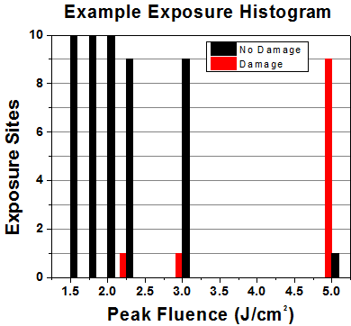
| Example Test Data | |||
|---|---|---|---|
| Fluence | # of Tested Locations | Locations with Damage | Locations Without Damage |
| 1.50 J/cm2 | 10 | 0 | 10 |
| 1.75 J/cm2 | 10 | 0 | 10 |
| 2.00 J/cm2 | 10 | 0 | 10 |
| 2.25 J/cm2 | 10 | 1 | 9 |
| 3.00 J/cm2 | 10 | 1 | 9 |
| 5.00 J/cm2 | 10 | 9 | 1 |
According to the test, the damage threshold of the mirror was 2.00 J/cm2 (532 nm, 10 ns pulse, 10 Hz, Ø0.803 mm). Please keep in mind that these tests are performed on clean optics, as dirt and contamination can significantly lower the damage threshold of a component. While the test results are only representative of one coating run, Thorlabs specifies damage threshold values that account for coating variances.
Continuous Wave and Long-Pulse Lasers
When an optic is damaged by a continuous wave (CW) laser, it is usually due to the melting of the surface as a result of absorbing the laser's energy or damage to the optical coating (antireflection) [1]. Pulsed lasers with pulse lengths longer than 1 µs can be treated as CW lasers for LIDT discussions.
When pulse lengths are between 1 ns and 1 µs, laser-induced damage can occur either because of absorption or a dielectric breakdown (therefore, a user must check both CW and pulsed LIDT). Absorption is either due to an intrinsic property of the optic or due to surface irregularities; thus LIDT values are only valid for optics meeting or exceeding the surface quality specifications given by a manufacturer. While many optics can handle high power CW lasers, cemented (e.g., achromatic doublets) or highly absorptive (e.g., ND filters) optics tend to have lower CW damage thresholds. These lower thresholds are due to absorption or scattering in the cement or metal coating.

LIDT in linear power density vs. pulse length and spot size. For long pulses to CW, linear power density becomes a constant with spot size. This graph was obtained from [1].
Pulsed lasers with high pulse repetition frequencies (PRF) may behave similarly to CW beams. Unfortunately, this is highly dependent on factors such as absorption and thermal diffusivity, so there is no reliable method for determining when a high PRF laser will damage an optic due to thermal effects. For beams with a high PRF both the average and peak powers must be compared to the equivalent CW power. Additionally, for highly transparent materials, there is little to no drop in the LIDT with increasing PRF.
In order to use the specified CW damage threshold of an optic, it is necessary to know the following:
- Wavelength of your laser
- Beam diameter of your beam (1/e2)
- Approximate intensity profile of your beam (e.g., Gaussian)
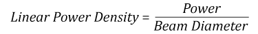
- Linear power density of your beam (total power divided by 1/e2 beam diameter)
Thorlabs expresses LIDT for CW lasers as a linear power density measured in W/cm. In this regime, the LIDT given as a linear power density can be applied to any beam diameter; one does not need to compute an adjusted LIDT to adjust for changes in spot size, as demonstrated by the graph to the right. Average linear power density can be calculated using the equation below.
The calculation above assumes a uniform beam intensity profile. You must now consider hotspots in the beam or other non-uniform intensity profiles and roughly calculate a maximum power density. For reference, a Gaussian beam typically has a maximum power density that is twice that of the uniform beam (see lower right).
Now compare the maximum power density to that which is specified as the LIDT for the optic. If the optic was tested at a wavelength other than your operating wavelength, the damage threshold must be scaled appropriately. A good rule of thumb is that the damage threshold has a linear relationship with wavelength such that as you move to shorter wavelengths, the damage threshold decreases (i.e., a LIDT of 10 W/cm at 1310 nm scales to 5 W/cm at 655 nm):
While this rule of thumb provides a general trend, it is not a quantitative analysis of LIDT vs wavelength. In CW applications, for instance, damage scales more strongly with absorption in the coating and substrate, which does not necessarily scale well with wavelength. While the above procedure provides a good rule of thumb for LIDT values, please contact Tech Support if your wavelength is different from the specified LIDT wavelength. If your power density is less than the adjusted LIDT of the optic, then the optic should work for your application.
Please note that we have a buffer built in between the specified damage thresholds online and the tests which we have done, which accommodates variation between batches. Upon request, we can provide individual test information and a testing certificate. The damage analysis will be carried out on a similar optic (customer's optic will not be damaged). Testing may result in additional costs or lead times. Contact Tech Support for more information.
Pulsed Lasers
As previously stated, pulsed lasers typically induce a different type of damage to the optic than CW lasers. Pulsed lasers often do not heat the optic enough to damage it; instead, pulsed lasers produce strong electric fields capable of inducing dielectric breakdown in the material. Unfortunately, it can be very difficult to compare the LIDT specification of an optic to your laser. There are multiple regimes in which a pulsed laser can damage an optic and this is based on the laser's pulse length. The highlighted columns in the table below outline the relevant pulse lengths for our specified LIDT values.
Pulses shorter than 10-9 s cannot be compared to our specified LIDT values with much reliability. In this ultra-short-pulse regime various mechanics, such as multiphoton-avalanche ionization, take over as the predominate damage mechanism [2]. In contrast, pulses between 10-7 s and 10-4 s may cause damage to an optic either because of dielectric breakdown or thermal effects. This means that both CW and pulsed damage thresholds must be compared to the laser beam to determine whether the optic is suitable for your application.
| Pulse Duration | t < 10-9 s | 10-9 < t < 10-7 s | 10-7 < t < 10-4 s | t > 10-4 s |
|---|---|---|---|---|
| Damage Mechanism | Avalanche Ionization | Dielectric Breakdown | Dielectric Breakdown or Thermal | Thermal |
| Relevant Damage Specification | No Comparison (See Above) | Pulsed | Pulsed and CW | CW |
When comparing an LIDT specified for a pulsed laser to your laser, it is essential to know the following:
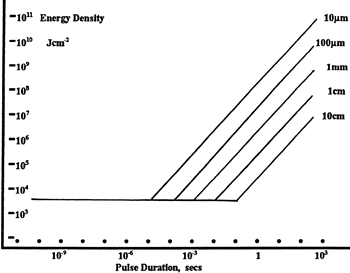
LIDT in energy density vs. pulse length and spot size. For short pulses, energy density becomes a constant with spot size. This graph was obtained from [1].
- Wavelength of your laser
- Energy density of your beam (total energy divided by 1/e2 area)
- Pulse length of your laser
- Pulse repetition frequency (prf) of your laser
- Beam diameter of your laser (1/e2 )
- Approximate intensity profile of your beam (e.g., Gaussian)
The energy density of your beam should be calculated in terms of J/cm2. The graph to the right shows why expressing the LIDT as an energy density provides the best metric for short pulse sources. In this regime, the LIDT given as an energy density can be applied to any beam diameter; one does not need to compute an adjusted LIDT to adjust for changes in spot size. This calculation assumes a uniform beam intensity profile. You must now adjust this energy density to account for hotspots or other nonuniform intensity profiles and roughly calculate a maximum energy density. For reference a Gaussian beam typically has a maximum energy density that is twice that of the 1/e2 beam.
Now compare the maximum energy density to that which is specified as the LIDT for the optic. If the optic was tested at a wavelength other than your operating wavelength, the damage threshold must be scaled appropriately [3]. A good rule of thumb is that the damage threshold has an inverse square root relationship with wavelength such that as you move to shorter wavelengths, the damage threshold decreases (i.e., a LIDT of 1 J/cm2 at 1064 nm scales to 0.7 J/cm2 at 532 nm):
You now have a wavelength-adjusted energy density, which you will use in the following step.
Beam diameter is also important to know when comparing damage thresholds. While the LIDT, when expressed in units of J/cm², scales independently of spot size; large beam sizes are more likely to illuminate a larger number of defects which can lead to greater variances in the LIDT [4]. For data presented here, a <1 mm beam size was used to measure the LIDT. For beams sizes greater than 5 mm, the LIDT (J/cm2) will not scale independently of beam diameter due to the larger size beam exposing more defects.
The pulse length must now be compensated for. The longer the pulse duration, the more energy the optic can handle. For pulse widths between 1 - 100 ns, an approximation is as follows:
Use this formula to calculate the Adjusted LIDT for an optic based on your pulse length. If your maximum energy density is less than this adjusted LIDT maximum energy density, then the optic should be suitable for your application. Keep in mind that this calculation is only used for pulses between 10-9 s and 10-7 s. For pulses between 10-7 s and 10-4 s, the CW LIDT must also be checked before deeming the optic appropriate for your application.
Please note that we have a buffer built in between the specified damage thresholds online and the tests which we have done, which accommodates variation between batches. Upon request, we can provide individual test information and a testing certificate. Contact Tech Support for more information.
[1] R. M. Wood, Optics and Laser Tech. 29, 517 (1998).
[2] Roger M. Wood, Laser-Induced Damage of Optical Materials (Institute of Physics Publishing, Philadelphia, PA, 2003).
[3] C. W. Carr et al., Phys. Rev. Lett. 91, 127402 (2003).
[4] N. Bloembergen, Appl. Opt. 12, 661 (1973).

In order to illustrate the process of determining whether a given laser system will damage an optic, a number of example calculations of laser induced damage threshold are given below. For assistance with performing similar calculations, we provide a spreadsheet calculator that can be downloaded by clicking the button to the right. To use the calculator, enter the specified LIDT value of the optic under consideration and the relevant parameters of your laser system in the green boxes. The spreadsheet will then calculate a linear power density for CW and pulsed systems, as well as an energy density value for pulsed systems. These values are used to calculate adjusted, scaled LIDT values for the optics based on accepted scaling laws. This calculator assumes a Gaussian beam profile, so a correction factor must be introduced for other beam shapes (uniform, etc.). The LIDT scaling laws are determined from empirical relationships; their accuracy is not guaranteed. Remember that absorption by optics or coatings can significantly reduce LIDT in some spectral regions. These LIDT values are not valid for ultrashort pulses less than one nanosecond in duration.
A Gaussian beam profile has about twice the maximum intensity of a uniform beam profile.
CW Laser Example
Suppose that a CW laser system at 1319 nm produces a 0.5 W Gaussian beam that has a 1/e2 diameter of 10 mm. A naive calculation of the average linear power density of this beam would yield a value of 0.5 W/cm, given by the total power divided by the beam diameter:
However, the maximum power density of a Gaussian beam is about twice the maximum power density of a uniform beam, as shown in the graph to the right. Therefore, a more accurate determination of the maximum linear power density of the system is 1 W/cm.
An AC127-030-C achromatic doublet lens has a specified CW LIDT of 350 W/cm, as tested at 1550 nm. CW damage threshold values typically scale directly with the wavelength of the laser source, so this yields an adjusted LIDT value:
The adjusted LIDT value of 350 W/cm x (1319 nm / 1550 nm) = 298 W/cm is significantly higher than the calculated maximum linear power density of the laser system, so it would be safe to use this doublet lens for this application.
Pulsed Nanosecond Laser Example: Scaling for Different Pulse Durations
Suppose that a pulsed Nd:YAG laser system is frequency tripled to produce a 10 Hz output, consisting of 2 ns output pulses at 355 nm, each with 1 J of energy, in a Gaussian beam with a 1.9 cm beam diameter (1/e2). The average energy density of each pulse is found by dividing the pulse energy by the beam area:
As described above, the maximum energy density of a Gaussian beam is about twice the average energy density. So, the maximum energy density of this beam is ~0.7 J/cm2.
The energy density of the beam can be compared to the LIDT values of 1 J/cm2 and 3.5 J/cm2 for a BB1-E01 broadband dielectric mirror and an NB1-K08 Nd:YAG laser line mirror, respectively. Both of these LIDT values, while measured at 355 nm, were determined with a 10 ns pulsed laser at 10 Hz. Therefore, an adjustment must be applied for the shorter pulse duration of the system under consideration. As described on the previous tab, LIDT values in the nanosecond pulse regime scale with the square root of the laser pulse duration:
This adjustment factor results in LIDT values of 0.45 J/cm2 for the BB1-E01 broadband mirror and 1.6 J/cm2 for the Nd:YAG laser line mirror, which are to be compared with the 0.7 J/cm2 maximum energy density of the beam. While the broadband mirror would likely be damaged by the laser, the more specialized laser line mirror is appropriate for use with this system.
Pulsed Nanosecond Laser Example: Scaling for Different Wavelengths
Suppose that a pulsed laser system emits 10 ns pulses at 2.5 Hz, each with 100 mJ of energy at 1064 nm in a 16 mm diameter beam (1/e2) that must be attenuated with a neutral density filter. For a Gaussian output, these specifications result in a maximum energy density of 0.1 J/cm2. The damage threshold of an NDUV10A Ø25 mm, OD 1.0, reflective neutral density filter is 0.05 J/cm2 for 10 ns pulses at 355 nm, while the damage threshold of the similar NE10A absorptive filter is 10 J/cm2 for 10 ns pulses at 532 nm. As described on the previous tab, the LIDT value of an optic scales with the square root of the wavelength in the nanosecond pulse regime:
This scaling gives adjusted LIDT values of 0.08 J/cm2 for the reflective filter and 14 J/cm2 for the absorptive filter. In this case, the absorptive filter is the best choice in order to avoid optical damage.
Pulsed Microsecond Laser Example
Consider a laser system that produces 1 µs pulses, each containing 150 µJ of energy at a repetition rate of 50 kHz, resulting in a relatively high duty cycle of 5%. This system falls somewhere between the regimes of CW and pulsed laser induced damage, and could potentially damage an optic by mechanisms associated with either regime. As a result, both CW and pulsed LIDT values must be compared to the properties of the laser system to ensure safe operation.
If this relatively long-pulse laser emits a Gaussian 12.7 mm diameter beam (1/e2) at 980 nm, then the resulting output has a linear power density of 5.9 W/cm and an energy density of 1.2 x 10⁻⁴ J/cm2 per pulse. This can be compared to the LIDT values for a WPQ10E-980 polymer zero-order quarter-wave plate, which are 5 W/cm for CW radiation at 810 nm and 5 J/cm2 for a 10 ns pulse at 810 nm. As before, the CW LIDT of the optic scales linearly with the laser wavelength, resulting in an adjusted CW value of 6 W/cm at 980 nm. On the other hand, the pulsed LIDT scales with the square root of the laser wavelength and the square root of the pulse duration, resulting in an adjusted value of 55 J/cm2 for a 1 µs pulse at 980 nm. The pulsed LIDT of the optic is significantly greater than the energy density of the laser pulse, so individual pulses will not damage the wave plate. However, the large average linear power density of the laser system may cause thermal damage to the optic, much like a high-power CW beam.
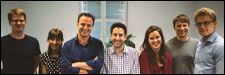 The team of researchers in Vienna, Austria.
About Thorlabs Crystalline Solutions
Crystalline Mirror Solutions (CMS) was founded in Vienna, Austria in 2012 by Drs. Garrett Cole and Markus Aspelmeyer. Their product offering was based on a spin-off of their fundamental research undertaken at the University of Vienna and the Vienna Center for Quantum Science and Technology. In the following year, CMS quickly expanded to include a site in Santa Barbara, California. Their single-crystal semiconductor supermirrors are a proprietary technology protected by international patents.
The application space of CMS’ novel coating technology spans optical components for ultraprecise optical clocks, precision interferometry, spectroscopy, as well as solutions for thermal management in high-power lasers and laser machining systems. Over the course of its history, CMS received a number of high-profile technology awards such as the Prism Award, the Leibinger Innovation Award, and the AMA Innovation Award, as well as various national and international start-up prizes. The organization’s supermirror technology was supported by the Defense Advanced Research Projects Agency (DARPA), the European Research Council, the Austrian Research Promotion Agency (FFG), and the Austria Wirtschaftsservice (aws).
Thorlabs acquired CMS in late 2019, adding their unique substrate-transferred single-crystal optical coating capabilities to its list of manufacturing competencies. The CMS team, which remains in Santa Barbara, is now known as Thorlabs Crystalline Solutions and is part of the Thorlabs Advanced Photonics group.
| Posted Comments: | |
user
(posted 2023-05-20 11:04:17.873) "Center Wavelength between 2.0 µm and 5.0 µm" -- What's preventing you from going to even longer wavelengths, up to the optical phonon frequency of GaAs/AlAs? It would be very useful to have a ~7-10 um supermirror. cdolbashian
(posted 2023-05-26 12:19:10.0) At the time of posting this, we are actively pursuing the development of supermirrors in such a wavelength range, but we have not yet evaluated the performance and feasibility of manufacturing such elements. I have contacted you directly to discuss this. |